
The $400 Million Machine Powering the Future of Chipmaking
BLUF: ASML unveiled a $400 million extreme‑ultraviolet (EUV) scanner that can pattern 7‑nanometer features at twice the speed of its predecessor, giving customers a faster path to 3‑nanometer and beyond, and tightening the supply chain for high‑performance chips.
What Is the $400 Million Machine?
It is ASML’s newest high‑NA EUV lithography platform, nicknamed “NXE:3400B”. The tool uses a 0.55 numerical aperture mirror to shrink the wavelength of light to 13.5 nm, enabling transistor gates under 5 nm. In practice it means chip fabs can print more transistors per wafer with fewer defects.
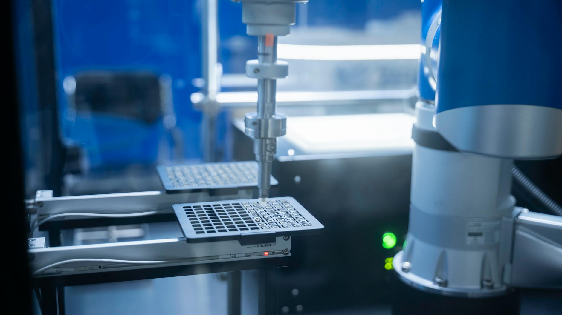
The machine occupies a 70‑meter cleanroom, consumes 400 kW of power, and costs roughly $400 million per unit. Only a handful of customers – TSMC, Samsung and Intel – have placed orders, but the ripple effect will be felt across every device that relies on silicon.
Why Does the $400 Million Machine Matter?
Semiconductor demand is outpacing supply, especially for AI accelerators and 5G smartphones. The new scanner shortens the gap between design and volume production, allowing manufacturers to stay ahead of Moore’s Law without massive redesign cycles. Governments that subsidize chip fabs see this as a strategic asset; the United States and EU have already earmarked billions to attract the tool.

Developers who build software for AI, gaming, or edge computing will notice performance gains as newer nodes become affordable faster. The machine also tightens the geopolitical balance – whoever controls the EUV supply chain can dictate pricing and access.
How Does the $400 Million Machine Work?
The core is a high‑NA reflective microscope. A laser‑generated plasma creates a cloud of tin droplets; when hit by a high‑energy pulse, the tin emits EUV photons. Mirrors coated with multilayer molybdenum/silicon reflect the light onto the wafer. The tool’s 0.55 NA lens focuses the beam to a spot size of 30 nm, far smaller than the 40 nm of previous models.
Advanced wafer‑stage robotics move the silicon at sub‑nanometer precision while a real‑time metrology system measures overlay errors. Software‑defined recipes adjust exposure dose on the fly, reducing defect density to below 0.1 defects per cm². The entire process is orchestrated by ASML’s proprietary YieldStar suite.
What Are the Downsides?
The price tag excludes all but the biggest fabs; smaller players must rely on older 193‑nm immersion tools, limiting their ability to compete on performance. The machine’s power draw adds to rising utility costs and carbon footprints, a concern for fabs aiming for sustainability certifications.

Supply chain bottlenecks for the custom mirrors and tin source mean lead times of 18‑24 months. Any disruption – such as a geopolitical embargo on critical components – could stall production across the whole industry.
Frequently Asked Questions
How many $400 million scanners are in operation?
As of Q2 2024, fewer than ten units have been shipped, all to TSMC, Samsung and Intel.
Will the machine reduce chip prices for consumers?
In the short term, prices stay high because the capital expense is passed to fabs, but faster yields eventually lower per‑chip costs.
What This Means
The $400 million EUV scanner is less a gadget and more a gatekeeper for the next wave of silicon. It accelerates the rollout of 3‑nanometer chips, but it also widens the gap between industry giants and niche players. Developers should watch roadmap announcements from TSMC and Samsung – the first silicon that runs on this tool will set performance baselines for AI and graphics for the next five years.
